
Micro-Electro-Mechanical Systems (MEMS) is a technology that integrates tiny mechanical elements, sensors, actuators, and electronics onto a single microchip.
Advanced microfabrication techniques often build these systems on a substrate, typically silicon, and fabricate them. MEMS technology widely uses these systems to create devices that have applications across various industries, including medical devices, consumer electronics, automotive, and aerospace.
The devices that make up MEMS typically range in size from 1 micron to several millimeters, making them incredibly small and efficient. These systems perform a variety of functions, including detecting environmental changes and initiating actions based on those changes.
In simple terms, MEMS combines the worlds of mechanical engineering and electronics into a single, tiny system capable of performing complex tasks.
Table of contents
What are Micro-Electro-Mechanical Systems (MEMS)?
At its core, MEMS refers to tiny devices that combine electrical and mechanical components. These devices have functional elements like sensors, actuators, and microelectronics, all miniaturized to a microscopic scale.
The most notable feature of MEMS devices is that they have at least one mechanical element, which could either move or be stationary. These elements perform specific functions, such as detecting environmental changes, processing data, and triggering actions based on this data.
For example, a MEMS accelerometer can sense acceleration and use that information to trigger an action in a system, like deploying airbags in a car. These systems are so small and integrated that people can use them in everyday devices, from smartphones to medical implants.
Other Names for MEMS
Different regions use different names for MEMS:
- In Japan, it’s often called Micromachines.
- In Europe, it’s known as Micro System Technology (MST).
- Other common terms include Microsensors, Microactuators, and Microtransducers.
Though the names vary, the core idea is the same: small-scale systems that combine mechanical and electronic functions.
History of MEMS
The idea of MEMS developed gradually over decades, shaped by many breakthroughs in science and engineering. Here’s a timeline of the most important milestones:
| Decade | Year | Event |
| 1940s–1960s: Early Discoveries | 1947 | Transistor invented at Bell Labs by William Shockley and team. |
| 1954 | Piezoresistive effect discovered in silicon and germanium. | |
| 1958–1959 | First integrated circuits (ICs) created by Jack Kilby and Robert Noyce. | |
| 1959 | Richard Feynman gave “There’s Plenty of Room at the Bottom” talk. | |
| 1959 | First silicon pressure sensor demonstrated. | |
| 1970s–1980s: MEMS Take Shape | 1971 | Microprocessor invented. |
| 1979 | HP developed micromachined inkjet nozzle (early MEMS product). | |
| 1982 | Silicon proposed as a structural material for mechanical devices. | |
| 1983 | Honeywell created integrated pressure and disposable medical sensors. | |
| 1985 | First crash sensors for airbags developed. | |
| 1990s: Industry Growth | 1991 | Carbon nanotube discovered. |
| 1993 | Texas Instruments launched digital micromirror device (DLP). | |
| 1993 | Analog Devices mass-produced surface micromachined accelerometers. | |
| 1994 | Bosch patented Deep Reactive Ion Etching (DRIE) process. |
How MEMS are Made?
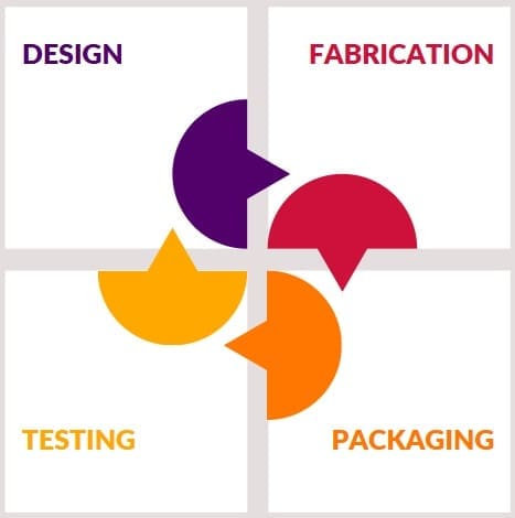
MEMS are manufactured using techniques similar to those used in making semiconductor chips. The process involves:
- Design
Engineers use special software tools to design MEMS layouts. These tools simulate mechanical movements and interactions between different components before someone physically creates the device. - Fabrication
This step uses micromachining to create tiny structures on silicon wafers. There are three major types of micromachining:- Bulk Micromachining
This technique involves etching directly into the silicon wafer to remove material and shape the device. The process is affected by the crystal structure of the silicon, which allows for precise geometries. - Surface Micromachining
Instead of etching into the wafer, this process builds structures layer by layer on top of the silicon. Engineers deposit multiple layers of material, and later remove some temporary layers (called sacrificial layers). This allows for the creation of complex, moving parts like hinges or gears. - High-Aspect-Ratio Micromachining (HAR)
This newer method allows for very tall and narrow features to be created with excellent precision. It uses thick layers of materials and advanced etching methods. It’s useful for devices that need large vertical structures, such as microturbines or complex optical elements.
- Bulk Micromachining
- Packaging
MEMS packaging protects the delicate structures from damage and keeps them working properly. Unlike typical electronics, MEMS packaging must also deal with mechanical strain, pressure, and environmental exposure. - Testing
Testing ensures that the MEMS devices function correctly. It is more complex than testing regular ICs because MEMS involve both electrical and mechanical parts. Advanced tools are used to simulate the operating environment and check the device’s reliability.
Characteristics of MEMS Fabrication

- Miniaturization
Because MEMS devices are so small, they react quickly and consume less energy. They can be placed in compact spaces and used in portable electronics and implants. Smaller size also often means faster response and higher sensitivity. - Multiplicity (Batch Fabrication)
Manufacturers produce MEMS in batches; they simultaneously make thousands or even millions of units on a single silicon wafer. This reduces the cost and allows for large-scale production. - Integration with Microelectronics
MEMS technology can combine sensors and mechanical structures directly with electronic circuits. This allows the creation of smart systems that can sense, process, and respond all on one chip. This integration is what makes MEMS so powerful and versatile.
What Is a Transducer in MEMS?
The MEMS field uses the general term “transducer” to describe any component that converts one form of energy into another. This includes both sensors (input devices) and actuators (output devices). For example, a pressure sensor converts mechanical pressure into an electrical signal, and a micro motor converts electrical energy into motion.
MEMS Operation
MEMS devices operate through a combination of mechanical, electrical, and sometimes even chemical interactions.
For instance, a MEMS accelerometer detects movement through the deflection of a small mass on a spring, which then triggers a sensor that sends data to the microelectronics for processing. Based on the data, the microelectronics can activate microactuators to perform a desired action.
The integration of sensors and actuators with electronics allows MEMS devices to respond in real-time to environmental changes. This feedback loop makes MEMS technology highly efficient and suitable for applications that require high precision and low power consumption.
Components of MEMS
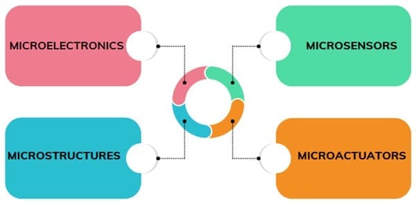
To understand MEMS more deeply, it’s crucial to explore its individual components:
- Microelectronics: The “brain” of the MEMS device, microelectronics are responsible for processing the data received from sensors. It makes decisions based on the information and controls the actuators to perform tasks.
- Microsensors: These components gather data from the environment. They can measure a range of physical properties like temperature, pressure, or magnetic fields. The data they collect is then sent to the microelectronics for processing.
- Microactuators: These are the components responsible for performing an action based on the processed information. For instance, an actuator could trigger a device to move or activate a mechanism.
- Microstructures: These are miniature mechanical components built directly onto the silicon chip. They are the structural elements that make MEMS devices functional, such as levers, gears, and pistons.
Fabrication of MEMS

Creating MEMS primarily focuses on microfabrication techniques and involves a series of complex manufacturing steps. These steps include deposition, patterning, and etching, each of which plays a vital role in shaping the final product.
Deposition: In this process, a thin layer of material is deposited onto the substrate. The material can vary depending on the requirements of the device and may include polysilicon, silicon dioxide, silicon nitride, or metals. Deposition techniques include physical methods like sputtering and evaporation or chemical methods such as chemical vapor deposition (CVD).
Patterning: After deposition, someone transfers a pattern onto the material. This pattern typically guides the etching process. Photolithography, a common technique, uses light to etch designs onto the material, thus patterning it.
Etching: The etching process removes unwanted material from the substrate. Two main types of etching exist: wet etching, where a chemical solution removes material by dipping the substrate, and dry etching, where gases or plasmas etch away the material.
Bonding: In some MEMS devices, multiple layers require bonding. Techniques like wafer bonding bond these layers together; in this process, two or more silicon wafers fuse to create a complex structure.
MEMS Fabrication Methods

Several methods are used to fabricate MEMS devices, each with its advantages and limitations:
- Bulk Micromachining: This is one of the oldest methods for fabricating MEMS and involves removing material from the bulk substrate (typically silicon) to create mechanical components. Wet etching is commonly used for this purpose.
- Surface Micromachining: This technique involves building up layers of material on the substrate and then removing sacrificial layers to leave behind functional mechanical structures. Surface micromachining allows for higher integration densities and lower production costs compared to bulk micromachining.
- Wafer Bonding: This method involves bonding two or more wafers together to create a composite structure. TTechniques like anodic bonding, intermediate layer bonding, or direct bonding can accomplish the bonding.
- High Aspect Ratio Fabrication: This involves etching very deep, narrow features into a substrate, allowing for the creation of high aspect ratio structures. This method is often used for creating 3D MEMS devices with vertical features.
How MEMS Operate?
MEMS operate by integrating mechanical structures with sensors and actuators, all controlled by microelectronics. The sensors detect physical changes in the environment, such as temperature or pressure, and send this information to the microelectronics.
The microelectronics process this data and signal the actuators to take an action, such as moving a mechanical part or triggering another device.
For instance, in a MEMS accelerometer (used in airbags), the sensor detects changes in acceleration, and the microelectronics process the data to trigger the actuator, which deploys the airbag in case of a collision.
Applications of MEMS
MEMS technology has found widespread use across numerous industries due to its small size, efficiency, and versatility. Some common applications include:
Automotive Industry: Vehicles use MEMS sensors for various functions, including airbag deployment, tire pressure monitoring, and stability control systems.
Medical Devices: Medical devices widely use MEMS in applications such as pacemakers, drug delivery systems, and pressure sensors for monitoring blood pressure.
Consumer Electronics: MEMS are integral to the functioning of smartphones, tablets, and other devices. Accelerometers, gyroscopes, and microphones use them, enabling features like motion sensing and touch controls.
Aerospace and Defense: Navigation systems, sensors for missile guidance, and other applications where precise and compact components are essential use MEMS technology.
Environmental Monitoring: MEMS sensors are used to monitor environmental conditions such as air quality, temperature, and humidity.
Industrial Automation: Industrial equipment can employ MEMS for monitoring systems, controlling actuators, and improving precision in manufacturing processes.
Key Concepts of MEMS
- Integration of Microelectronics and Mechanics: MEMS integrates electronic and mechanical components on a single chip.
- Microfabrication Techniques: MEMS devices are created using advanced fabrication methods like deposition, patterning, and etching.
- Sensors and Actuators: MEMS rely on sensors to detect environmental changes and actuators to respond to those changes.
- Small Scale: MEMS devices are typically microscopic, which allows them to be used in a wide range of applications without taking up much space.
- Versatility: MEMS technology has applications in a variety of industries, including automotive, healthcare, aerospace, and consumer electronics.
Final Words
MEMS (Micro-Electro-Mechanical Systems) is a revolutionary technology that combines microelectronics, mechanical structures, and sensors to create compact, efficient devices.
The process of creating MEMS involves intricate fabrication techniques like deposition, patterning, and etching. Through these processes, tiny mechanical systems are created that can sense changes in the environment and take appropriate actions.
The applications of MEMS are vast, from automotive safety to medical devices, and its potential continues to grow as more industries recognize the benefits of using miniature, efficient systems. However, challenges remain in terms of scalability, material properties, and cost, but the future of MEMS looks promising as the technology continues to evolve.